Executive Summary: The Engines of Modern Computation
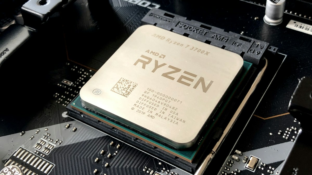
At the heart of every digital computing device—from smartwatches and smartphones to supercomputers and artificial intelligence data centers—reside semiconductor microprocessors. For decades, the undisputed king of silicon was the Central Processing Unit (CPU), celebrated as the “brain” of the computer.
However, in the modern computing landscape, the Graphics Processing Unit (GPU) has experienced a historic, unprecedented ascendance. Once regarded as specialized add-in cards intended solely for rendering 3D video game polygons, GPUs have become the foundational computational substrate powering the modern Artificial Intelligence revolution, scientific molecular simulations, cryptocurrency cryptography, and autonomous vehicle perception.
Understanding the deep microarchitectural, mathematical, and philosophical differences between a CPU and a GPU is essential for understanding how modern computers work and why semiconductor engineering has become the geopolitical fulcrum of the global economy.
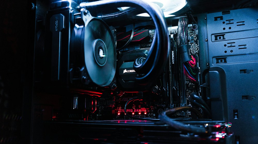 Figure 1: Silicon photolithography: Transistor scaling across 3nm FinFET and Gate-All-Around (GAA) architectures.
1. Philosophical Distinction: Latency vs. Throughput
The fundamental divergence between a CPU and a GPU stems from two radically opposing design philosophies:
+--------------------------------------------------------------+
|                     CPU vs. GPU PHILOSOPHY                   |
+------------------------------+-------------------------------+
| CENTRAL PROCESSING UNIT (CPU)| GRAPHICS PROCESSING UNIT (GPU)|
+------------------------------+-------------------------------+
| - Optimized for LOW LATENCY  | - Optimized for HIGH          |
| - Few complex, powerful cores|   THROUGHPUT                  |
| - Master of SEQUENTIAL logic | - Thousands of small, simple  |
| - "A sports car carrying a   |   arithmetic cores            |
|   single package at 200 mph" | - Master of PARALLEL math     |
|                              | - "A 100-car train carrying   |
|                              |   10,000 packages at 50 mph"  |
+------------------------------+-------------------------------+- The CPU is optimized to execute a single, complex thread of instructions as rapidly as humanly possible. It excels at unpredictable, branching sequential logic: running an operating system kernel, parsing an arbitrary JavaScript file, managing filesystem I/O, and handling user mouse interrupts.
- The GPU is optimized to execute millions of identical, independent mathematical operations simultaneously. It does not care about how quickly an individual operation completes; it cares about total computational throughput per clock cycle.
2. Microarchitecture Breakdown: Die Real Estate
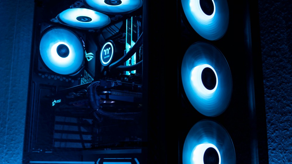 Figure 2: Microarchitecture contrast: CPU optimized for latency-critical branch prediction versus GPU throughput parallelism.
If you inspect a modern silicon die under an electron microscope, the physical layout reveals why their capabilities differ so sharply:
The Anatomy of a CPU Core
In a modern CPU (Intel Core Ultra, AMD Ryzen, Apple M-series), only a minor fraction of the silicon area is dedicated to raw Arithmetic Logic Units (ALUs). The vast majority of the die real estate is consumed by complex control logic and cache memory:
- Branch Predictors & Speculative Execution Units: Massive neural-like circuits that predict which direction an
if-elsecondition will take before it is evaluated, executing code ahead of time to eliminate pipeline stalls. - Out-of-Order Execution (OoO) Engines: Specialized logic that reorders linear instructions on the fly to maximize ALU utilization.
- Massive Multi-Tier Cache Hierarchy (L1, L2, L3): Gigabytes of ultra-low latency SRAM sitting directly beside the cores, shielding the processor from slow external DRAM latency.
The Anatomy of a GPU
A GPU (NVIDIA Blackwell, AMD RDNA/CDNA) discards almost all of this complex control circuitry:
- It possesses minimal branch prediction and simplified out-of-order execution logic.
- Instead, over 80% of the silicon area is dedicated to vast, repeating arrays of ALUs (Compute Cores).
- A flagship CPU possesses 16 to 24 cores. A flagship GPU possesses over 16,000 CUDA/Stream cores operating in parallel.
- GPUs operate on the SIMD (Single Instruction, Multiple Data) or SIMT (Single Instruction, Multiple Threads) paradigm: a single control instruction is broadcast to thousands of cores, each executing the identical arithmetic formula on a different set of numbers simultaneously.
3. Mathematical Foundations: Linear Algebra and Matrix Multiplication
Why did GPUs conquer the artificial intelligence and machine learning revolution? The answer lies in Linear Algebra.
The Mathematics of Graphics (3D Rendering)
To render a 3D video game scene, the computer represents virtual 3D objects as geometric meshes composed of millions of triangles. To project these triangles onto a flat 2D monitor screen, apply lighting shadows, and rotate camera angles, the computer must execute 4x4 matrix transformations and vector dot products on every vertex and pixel, 60 to 120 times every second:
$$\begin{bmatrix} x’ \ y’ \ z’ \ 1 \end{bmatrix} = \begin{bmatrix} m_{00} & m_{01} & m_{02} & m_{03} \ m_{10} & m_{11} & m_{12} & m_{13} \ m_{20} & m_{21} & m_{22} & m_{23} \ 0 & 0 & 0 & 1 \end{bmatrix} \begin{bmatrix} x \ y \ z \ 1 \end{bmatrix}$$
A CPU would have to process these millions of matrix multiplications sequentially, resulting in an unplayable slideshow of 2 frames per second. A GPU executes thousands of these dot products concurrently, delivering 144 frames per second effortlessly.
The Serendipitous AI Convergence
In the early 2010s, deep learning pioneers (including Alex Krizhevsky and Geoffrey Hinton in the landmark 2012 ImageNet paper) realized an astonishing mathematical convergence:
- An artificial neural network layer is mathematically identical to a massive matrix multiplication!
- Computing forward activations involves multiplying an input vector by a weight matrix: $\vec{a} = \sigma(W \vec{x} + \vec{b})$.
- Training an LLM with hundreds of billions of parameters requires executing trillions of General Matrix Multiplications (GEMM).
- The GPU was already the world’s most perfected matrix multiplication engine. Overnight, graphics accelerators became the computational foundation of artificial intelligence.
4. The Memory Bandwidth Bottleneck: DDR5 vs. GDDR6 / HBM3
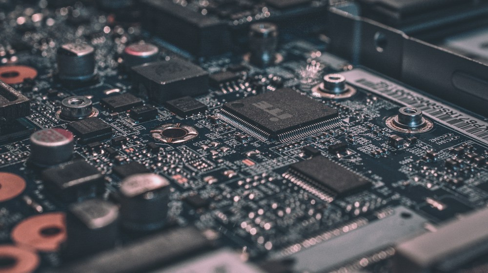 Figure 3: Memory bandwidth bottleneck: High Bandwidth Memory (HBM3e) delivering terabytes per second to parallel tensor cores.
Computational cores are useless if they sit starved of data. The divide between CPU and GPU manifests acutely in memory architecture:
| Memory Specification | Modern Desktop CPU (DDR5) | Modern Enterprise GPU (HBM3e) |
|---|---|---|
| Bus Width | 128-bit dual-channel | 4096-bit ultra-wide 3D stacked bus |
| Peak Memory Bandwidth | ~80 to 100 GB/second | Over 8,000 GB/second (8 TB/s) |
| Memory Latency | Ultra-Low (~50 to 70 nanoseconds) | Higher (~150 to 250 nanoseconds) |
| Primary Goal | Minimize time to fetch a single pointer | Maximize continuous volume of gigabytes per clock |
A CPU relies on low-latency memory to fetch pointers and jump between branches instantly. A GPU accepts higher latency in exchange for an immense firehose of High Bandwidth Memory (HBM), flooding thousands of parallel cores with matrix weights simultaneously.
5. Architectural Comparison Matrix
| Architectural Feature | Central Processing Unit (CPU) | Graphics Processing Unit (GPU) |
|---|---|---|
| Core Count | 4 to 32 powerful, complex cores | 2,000 to 18,000 specialized parallel cores |
| Instruction Execution | Sequential, Out-of-Order (OoO) | Massively Parallel, SIMD / SIMT |
| Clock Frequency | High (3.5 GHz to 6.0 GHz) | Lower (1.5 GHz to 2.8 GHz) |
| Branching Efficiency | Highly efficient; advanced branch prediction | Inefficient; branch divergence causes execution stalls |
| Optimal Workloads | Operating systems, web servers, databases, compilers | 3D graphics, neural networks, crypto, physics simulations |
| Programming Model | C, C++, Rust, Python, Go, Java | CUDA, OpenCL, Metal, Vulkan, ROCm |
Conclusion: The Era of Heterogeneous Computing
The historical rivalry between the CPU and GPU has culminated not in the elimination of either, but in their intimate symbiosis: Heterogeneous System Architecture (HSA).
In modern smartphones (Apple A-series/M-series, Qualcomm Snapdragon) and modern enterprise AI servers (NVIDIA Grace Hopper), the CPU and GPU are fabricated on the identical silicon substrate or unified interposer, sharing a pool of unified, high-speed memory. The CPU acts as the master orchestrator, managing operating system processes, disk I/O, and user interaction, while seamlessly dispatching massive matrix operations to the GPU and dedicated Neural Processing Units (NPUs). Mastering the distinct capabilities of both processors is the prerequisite for designing the next generation of high-performance software.
The Rise of NPUs and Specialized Domain-Specific Accelerators
Beyond the classic CPU and GPU duality, modern silicon engineering has entered the era of heterogeneous computing dominated by Neural Processing Units (NPUs) and Domain-Specific Architectures (DSAs).
While GPUs excel at dense 32-bit floating point matrix math required for training foundational models, running inference efficiently on consumer edge devices—such as laptops and smartphones—requires specialized low-power acceleration. NPUs are custom-tailored for low-precision 8-bit and 4-bit integer quantization (INT8/INT4), executing billions of neural network operations per second while drawing mere milliwatts of battery power.
+--------------------------------------------------------------+
|            Modern Heterogeneous System-on-Chip (SoC)         |
+--------------------------------------------------------------+
| [High-Performance CPU Cores]  -> OS, Logic, Single-Thread    |
| [Efficiency CPU Cores]        -> Background Tasks, Idle      |
| [Multi-Core GPU]              -> Rendering, Shaders, 3D      |
| [Neural Engine / NPU]         -> Local LLM, Voice, Vision    |
| [Unified Memory Architecture] -> Zero-Copy RAM Interconnect  |
+--------------------------------------------------------------+
By placing high-bandwidth unified memory pools between CPU, GPU, and NPU cores on a single physical die, modern System-on-Chip (SoC) designs eliminate costly PCIe bus copy latencies, unlocking real-time generative intelligence on everyday consumer devices.


How Smartphones Have Evolved Over the Years
A comprehensive technological history tracing the smartphone evolution from early cellular communicators to multi-camera silicon powerhouses and on-device neural engines.

OLED vs AMOLED vs LCD: Understanding Display Technologies
A comprehensive optical engineering comparison of LCD, OLED, and AMOLED display panels, evaluating backlights, organic semiconductors, contrast ratios, burn-in, and power efficiency.
How Wi-Fi 7 Is Changing Wireless Connectivity
A deep technical investigation into Wi-Fi 7 (IEEE 802.11be), examining 320 MHz channel widths, 4096-QAM, Multi-Link Operation (MLO), deterministic latency, and 46 Gbps theoretical throughput.